
黑琵與白琵2012.01.15三民-張清桐

反嘴長腳鷸(反嘴鴴)

小秋沙(白秋沙)-石明卿

黃鸝-張清桐2011.09

小椋鳥,絲光,灰山椒,壽帶-石明卿2011.09
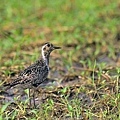
金斑鴴-邱建福

Spoonbill-姚書寰

黑冠鵑隼和松雀鷹打架1-林文宏

3五色鳥-石明卿

2環頸雉-石明卿

1池鷺-石明卿

黑冠鵑隼-黃家發2011.09.18

黑冠鵑隼-黃家發2011.09.18

黑冠鵑隼-黃家發2011.09.18
黑冠鵑隼-黃家發2011.09.18

赤腹鷹群-黃家發
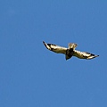
毛足鵟-2011.8姚書寰

金翼白眉-黃家發

白眉林鴝-黃家發

台灣山鷓鴣-黃家發

藍腹鷳-黃家發

黑長尾雉-黃家發

黑長尾雉(公)-黃家發

黑長尾雉-黃家發攝.bmp

黑長尾雉-黃家發攝.bmp
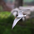
小燕鷗-石明卿
吞食吳郭魚-石明卿
獵獲吳郭魚-石明卿

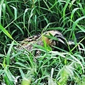
靜待獵物-石明卿

移動時的姿態-石明卿

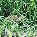
在草叢中擬態-石明卿

male Orange-breasted Trogon-Amorn.jpg

八色鳥

A21-Yellow-vented Bulbuln1.jpg石明卿

A19-Asian Glossy Starling 亞洲輝椋鳥.jpg 石明卿

A17-Oriental Magpie-robin 鵲鴝.jpg石明卿
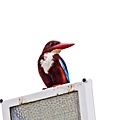
A15-White-throated Kingfisher 白胸翡翠.jpg石明卿
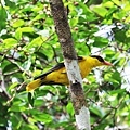
C12-Black-caped Oriole 黃鸝.jpg石明卿
繫放-許育誠

繫放0-許育誠

黑尾鷸(足旗) 20110423

栗小鷺-石明卿

灰面鵟鷹-石明卿

紅隼-石明卿

紅胸鴴 01-石明卿

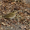
赤喉鹨-石明卿

燕鴴-石明卿

棕頭鴉雀(粉紅鶯嘴)-石明卿

紅頭潛鴨-黃家發

黃雀-張耀文

黃雀-張耀文

紅背伯勞-張清桐

紅胸鴴-張清桐

壽帶鳥-張清桐

紫壽帶公鳥-張清桐

birds of Boneo

birds of Boneo

小鸊鷉白子2-藍振峰

小鸊鷉白子1-藍振峰

birds-1

黃尾鴝-藍振峰

黃山雀-藍振峰

巨嘴鴉入侵喜鵲巢 -石明卿

喜鵲與巢-石明卿

喜鵲啣枝築巢-石明卿

喜鵲02-石明卿

喜鵲 01- 石明卿

翹鼻麻鴨 (花鳧)-石明卿

白額雁亞成鳥02-石明卿
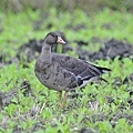
白額雁亞成鳥01-石明卿

黑頸鷿鷉- 石明卿

台灣獼猴-石明卿
樹鹨-石明卿

黑冠麻鷺-石明卿

黃尾鴝(雄)-石明卿

黃山雀-石明卿

紅頭山雀-石明卿

紫嘯鶇-石明卿

冠羽畫眉02-石明卿

冠羽畫眉01-石明卿

相片最新留言
-
 盧沛丞(雄中小明)教味之堡早餐店高雄市鳳山區過埤里田衙路157號1樓 物理 說:Witness for the Prosecution...
 -
 林鳳竹 說:請問,可以使用這張圖嗎?
 -
林鳳竹 說:請問,可以使用這張圖嗎?
-

-
 智明 彭 說:請問石教授這張照片是哪一年...
此相簿內的相片出現在:
相簿列表資訊
- 最新上傳:
- 2015/03/31
- 全站分類:
- 創作設計
- 本日人氣:
- 0
- 累積人氣:
- 18182

張張都美麗動人!那羽長尾濶嘴鳥應該是馬來西亞拍到的吧!?
常見的半導體材料有矽、鍺、砷化鎵等
/
晶片測試
晶片處理高度有序化的本質增加了對不同處理步驟之間度量方法的需求。晶片測試度量裝置被用於檢驗晶片仍然完好且沒有被前面的處理步驟損壞。如果If the number of dies—the 積體電路s that will eventually become chips—當一塊晶片測量失敗次數超過一個預先設定的閾值時,晶片將被廢棄而非繼續後續的處理製程。
/
晶片測試
晶片處理高度有序化的本質增加了對不同處理步驟之間度量方法的需求。晶片測試度量裝置被用於檢驗晶片仍然完好且沒有被前面的處理步驟損壞。如果If the number of dies—the 積體電路s that will eventually become chips—當一塊晶片測量失敗次數超過一個預先設定的閾值時,晶片將被廢棄而非繼續後續的處理製程。
/
步驟列表
晶片處理
濕洗
平版照相術
光刻Litho
離子移植IMP
蝕刻(干法蝕刻、濕法蝕刻、電漿蝕刻)
熱處理
快速熱退火Annel
熔爐退火
熱氧化
化學氣相沉積 (CVD)
物理氣相沉積 (PVD)
分子束磊晶 (MBE)
電化學沉積 (ECD),見電鍍
化學機械平坦化 (CMP)
IC Assembly and Testing 封裝測試
Wafer Testing 晶片測試
Visual Inspection外觀檢測
Wafer Probing電性測試
FrontEnd 封裝前段
Wafer BackGrinding 晶背研磨
Wafer Mount晶圓附膜
Wafer Sawing晶圓切割
Die attachment上片覆晶
Wire bonding焊線
BackEnd 封裝後段
Molding模壓
Post Mold Cure後固化
De-Junk 去節
Plating 電鍍
Marking 列印
Trimform 成形
Lead Scan 檢腳
Final Test 終測
Electrical Test電性測試
Visual Inspection光學測試
Baking 烘烤
/
有害材料標誌
許多有毒材料在製造過程中被使用。這些包括:
有毒元素摻雜物比如砷、硼、銻和磷
有毒化合物比如砷化三氫、磷化氫和矽烷
易反應液體、例如過氧化氫、發煙硝酸、硫酸以及氫氟酸
工人直接暴露在這些有毒物質下是致命的。通常IC製造業高度自動化能幫助降低暴露於這一類物品的風險。
/
Device yield
Device yield or die yield is the number of working chips or dies on a wafer, given in percentage since the number of chips on a wafer (Die per wafer, DPW) can vary depending on the chips' size and the wafer's diameter. Yield degradation is a reduction in yield, which historically was mainly caused by dust particles, however since the 1990s, yield degradation is mainly caused by process variation, the process itself and by the tools used in chip manufacturing, although dust still remains a problem in many older fabs. Dust particles have an increasing effect on yield as feature sizes are shrunk with newer processes. Automation and the use of mini environments inside of production equipment, FOUPs and SMIFs have enabled a reduction in defects caused by dust particles. Device yield must be kept high to reduce the selling price of the working chips since working chips have to pay for those chips that failed, and to reduce the cost of wafer processing. Yield can also be affected by the design and operation of the fab.
Tight control over contaminants and the production process are necessary to increase yield. Contaminants may be chemical contaminants or be dust particles. "Killer defects" are those caused by dust particles that cause complete failure of the device (such as a transistor). There are also harmless defects. A particle needs to be 1/5 the size of a feature to cause a killer defect. So if a feature is 100 nm across, a particle only needs to be 20 nm across to cause a killer defect. Electrostatic electricity can also affect yield adversely. Chemical contaminants or impurities include heavy metals such as Iron, Copper, Nickel, Zinc, Chromium, Gold, Mercury and Silver, alkali metals such as Sodium, Potassium and Lithium, and elements such as Aluminum, Magnesium, Calcium, Chlorine, Sulfur, Carbon, and Fluorine. It is important for those elements to not remain in contact with the silicon, as they could reduce yield. Chemical mixtures may be used to remove those elements from the silicon; different mixtures are effective against different elements.
Several models are used to estimate yield. Those are Murphy's model, Poisson's model, the binomial model, Moore's model and Seeds' model. There is no universal model; a model has to be chosen based on actual yield distribution (the location of defective chips) For example, Murphy's model assumes that yield loss occurs more at the edges of the wafer (non-working chips are concentrated on the edges of the wafer), Poisson's model assumes that defective dies are spread relatively evenly across the wafer, and Seeds's model assumes that defective dies are clustered together.[25]
Smaller dies cost less to produce (since more fit on a wafer, and wafers are processed and priced as a whole), and can help achieve higher yields since smaller dies have a lower chance of having a defect. However, smaller dies require smaller features to achieve the same functions of larger dies or surpass them, and smaller features require reduced process variation and increased purity (reduced contamination) to maintain high yields. Metrology tools are used to inspect the wafers during the production process and predict yield, so wafers predicted to have too many defects may be scrapped to save on processing costs.[26]